
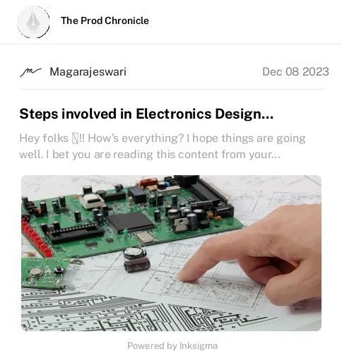


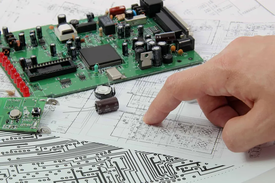
Hey folks 😃!! How’s everything? I hope things are going well. I bet you are reading this content from your mobile, laptop, or desktop. A hard guess right? 😉We all know these are electronic devices. Ever wondered about the process involved in manufacturing these devices? I am pretty much sure, you would have. I know you have been that small kid who had questions about everything around you. Well, you have found a post to understand it.
Process flow in electronics design and manufacturing:
Planning & Initial-Design --> Simulation, analysis --> Prototype testing and validation -->Design Iteration-->Design for manufacturing check --> BOM finalization --> Procurement--> PCBA-->Production, Testing
Planning, Initial Design, and Analysis:
Product development is an iterative process. It should require a proper plan and execution. Once a product development discussion starts, a list of features and functionalities that are supposed to be incorporated must be figured out. This will help in determining the feasibility, cost, resources, and timeline required for the project. Initial Design is done by either a single person or a team based on complexity. Then it is reviewed by a senior person. To save time, certain companies perform initial design verification with the help of third-party organizations that have a team of experienced professionals.
Major Semiconductor manufacturers like Texas Instruments, Power Integrations, Analog Devices, etc. have design tools, reference designs, and public forums to help design engineers. These resources have reduced the time, cost, and effort involved in the product development phase for many companies. It is better to simulate a design at different conditions to understand its performance rather than testing it using multiple prototypes. In addition to these resources, multiple sites provide open-source hardware designs developed by hobbyists and engineers around the world.
Prototype Testing and Validation:
This stage is where the design validation, component validation, and project feasibility are done. Previously prototype-level testing is done using perf boards and breadboards. This saves time but it has certain downsides like difficulties in rework, the inclusion of IC adaptors, and size constraints as THT parts are used.
Because of this engineers nowadays prefer PCB prototypes. This transition became possible as PCB manufacturing companies like JLC PCB provided prototypes at a significantly lower price at a faster rate. Once the prototype is built it is tested for functionality and behavior at various atmospheric conditions. This will help to iterate and improvise the design. Based on the testing the BOM will change. Usually, it is better to have as much as iterations as possible before moving into the production stage.
Pre-production phase:
There is a misconception among hobbyists and budding engineers that once prototype testing is done, the product is market ready. This is where the fun begins. Global chip shortage is driving the electronic market crazy. Many companies build their prototype with a chip and once it is ready for production, they are not able to purchase the IC for the production quantity. This is not specific to startups. Even multinational companies face this issue. So the BOM has to be checked carefully for the availability of the parts.
Finding the right EMS partner is another important step that has to be taken care of before production. Each EMS partner has a procedure for mass manufacturing. They will review the PCB design and will let you know in case of any Design for manufacturing (DFM) issues. This is done to improvise the process and reduce the time of manufacturing.
Production phase:
Once BOM and EMS partner is finalized, procurement has to be started. Some EMS partners support in procurement of parts too. It is better to check the quality and functionality of important IC and modules before moving into mass production. There are a lot of fake parts in the market. After this, the PCB assembly happens and the PCB is assembled in an enclosure of the product. It is then tested for its quality and functionality. Once all tests pass it is shipped out to the customer. There are multiple steps involved in PCB manufacturing which will be discussed in the upcoming blogs.


